Advanced Materials Characterisation
Meeting Materials 2022, the annual M2i conference, was organized in close collaboration with 4TU.HTM.
Keynote speakers:
- Prof. Cem Tasan (MIT): Hydrogen where are you?
- Prof. Mary Ryan (Imperial College London): Engineering nanomaterials for function and safety
- Prof. Peter Lee (UCL): Validating additive manufacturing models using in situ and operando synchronoton experiments
 M2i Meeting Materials 2022 took place on the 13th of December 2022. Thanks to all the speakers and to so many participants (link to Twitter feed including pictures) for joining the 4TU.HTM Advanced Materials Characterisation session.
We'll add pictures and presentations here.
- Presentation by Lars Bannenberg - TU Delft (3 MB)
X-ray and Neutron Diffraction and Reflectometry for (thin film) material characterization - Presentation by Martin Luckabauer - UTwente (3 MB)
High-precision dilatometry, precipitation processes in titanium and aluminum alloys - Presentation by Antonija Grubišić-Čabo - UG (86 MB)
Angle-Resolved Photoemission Spectroscopy for crystalline (two-dimensional) material characterization - Presentation by Sieger van der Laan - Tata Steel (12 MB)
Integrating microscopy (SEM, LOM) with elemental and phase mapping (EDS, LA-ICP-TOFMS, EBSD) - Presentation by Daniel Nijhof & Gesa Welker - TU Eindhoven / TU Delft (8 MB)
Smart*Light: A new type of X-ray source for materials characterization
Aim
The aim of this session is to bring together scientists from academia and industry applying all kinds of new and advanced materials characterisation techniques for characterisation purposes, for an exchange of ideas and observations both with each other and with the audience attending the Meeting Materials conference. These possible characterization purposes cover all types of materials within the field of materials science. The audience will involve university researchers, researchers from research institutes, and (R&D) representatives of companies, both large multi-national corporates as well as SMEs from a broad range of materials industries.
Speakers
Dr.ir. Marijn van Huis
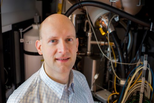 Debye Institute for Nanomaterials Science, Utrecht University
Title: Advanced Electron Microscopy for Steels and Alloys
Abstract
The engineering of novel materials increasingly takes place at the nanoscale. Electron microscopy (EM) is often the only method that can provide detailed structural and chemical characterization at the nanoscale, and offers an extensive toolbox of imaging and analytical techniques. In this talk I will highlight a few successes, and show new avenues ahead of us through which we can not only characterize the material, but also follow in time the processes taking place in the material during fabrication of during usage. This is achieved through so-called in-situ EM: performing experiments inside the electron microscope.
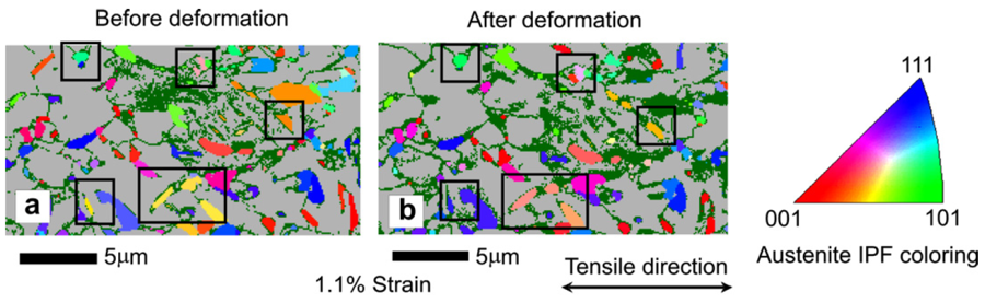
The first example is the precipitation in Al-Mg-Si alloys (AA6xxx series) where a whole sequence of transformations of the precipitates has been revealed by detailed high-resolution transmission electron microscopy (HR-TEM) and electron diffraction (ED) [1]. The formation of precipitates upon heating was also followed in-situ in the transmission electron microscope by heating a thin slab of an aluminum AA7xxx alloy; even a 3D reconstruction of the slab including the various precipitates was made using electron tomography [2]. Finally, using scanning electron microscopy (SEM) on multiphase steels, both the phase (ferrite, austenite, martensite) and the orientation of the phases in the microstructure can be mapped using electron backscatter diffraction (EBSD). By examing the same area of a TRIP steel before and after various stages of deformation, we revealed that austenite grains often undergo rotations before transforming into martensite [3], as shown in the Figure. The results have often been obtained in close collaboration with industrial partners, and we welcome new ideas and projects.
Marijn van Huis is an expert both in transmission electron microscopy (TEM) and density functional theory (DFT) calculations, and uses these experimental and simulation tools to study nanoparticles and nanocrystals with novel physical properties.
References
- J.H. Chen, E. Costan, M.A. van Huis, Q. Xu and H.W. Zandbergen, ‘Atomic pillar-based nanoprecipitates strengthen AlMgSi alloys’, Science 312 (2006) p. 416-419
- S.R.K. Malladi, Q. Xu, M.A. van Huis, F.D. Tichelaar, K. J. Batenburg, E. Yucelen, B. Dubiel, A. Czyrska-Filemonowicz, H.W. Zandbergen, ‘Real-time atomic scale imaging of microstructural evolution in alloys’, Nano Letters 14 (2014) 384-389
- G.K. Tirumalasetty, M.A. van Huis, C. Kwakernaak, J. Sietsma, W.G. Sloof and H.W. Zandbergen, ‘Deformation induced austenite grain rotation and transformation in TRIP assisted steel’, Acta Mater. 60 (2012) 1311-1321
Prof.dr. Sieger van der Laan
Scientific Fellow, Tata Steel & Professor Building Materials, Eindhoven University of Technology
Title: Integrating microscopy (SEM, LOM) with elemental and phase mapping (EDS, LA-ICP-TOFMS, EBSD)
The presentation is available here (12 MB)
Abstract - Correlative Data Fusion – Integrating Optical and Scanning Electron Imaging with elemental mapping by EDS and LA-ICP-TOFMS and crystallography by EBSD Selection of materials for purpose is generally based on their bulk properties for which measurement techniques are well established with routine protocols (e.g., from tensile & compressive strength testing of construction materials, to leaching properties of by-products). The bulk properties of materials, however, derive from the constituent phases and their spatial distribution. Thus, microstructures of materials are key to understand properties, and to enable development of novel materials. In this presentation, we will show how various techniques for microscopy and major and trace microanalysis can be integrated and what spatial and chemical resolution can be obtained.
Data fusion uses the complementary strengths of multiple methods to obtain new insights from correlations among the data sources, but this approach critically hinges on accurate and reliable spatial overlaying of the data layers. Recent advances now permit optical and back-scattered electron microscopy images to be matched within 100 nm, and to within 1-2 μm with element distribution images from EDS-microanalysis. State-of-the-art LA ICP-TOFMS (Laser-Ablation ICP-Time-of-Flight Mass Spectrometry) analysis can resolve the trace element spatial distribution down to 1 μm, and be similarly overlain with 1-2 μm accuracy. In addition, EBSD (Electron Back Scatter Diffraction) adds crystallographic information at < 100 nm to differentiate polymorphs and reveal preferred crystallographic orientation (texture). In the x-y plane, the various data sources can thus be overlain at their analytical spatial resolution. In the z direction, data are matched to 5-10 μm, which results from differences in sampled volume among the methods.
One of the main benefits of combining methods is the huge dynamic range obtained both spatially (cm to 100 nm, a 105 dynamic range) and chemically. Elemental detection limits for EDS-measured phase compositions can be as low as 0.1wt%, except for the light elements, Li, Be, B, C, N, O, and F. Complementary, LA ICP-TOFMS can routinely measure most elements down to sub-ppm level with 10% accuracy, and down to sub-ppb level for select elements at optimized conditions. This represents a 109 dynamic range in concentration and permits correlating major element behaviour with that of trace elements, and to simultaneously investigate elements that control the thermodynamic stability of a phase and those that are passive tracers of conditions and element provenance.
This suite of analytical techniques is universally applicable to all solid-state materials. In the presentation, application to a multi-phase oxide material (BOF-steel making slag) will be presented. The results are of relevance for the hydration behavior and leaching properties of slag and its potential to be developed as an alternative cementitious material.
Dr. Martin Luckabauer
Assistant Professor, Production Technology, Faculty of Engineering Technology, University of Twente
Title: High-precision dilatometry, precipitation processes in titanium and aluminum alloys (method and application)
Presentation by Martin Luckabauer (Pdf file)
 Abstract
During the last decades especially advancements in the field microscopic techniques, especially transmission electron microscopy and atom probe tomography, strongly improved the possibilities for the characterization of materials at the nano-scale. In contrast, standard methods for assessing the kinetics, e.g., the evolution of the volume fraction of a microstructural feature as a function of time, did not improve in the same way.
In principle, dilatometry, i.e., the measurement of the sample volume (or length) as a function of time and temperature is capable of detecting all kinetic phenomena in materials, since with rare exceptions every change in microstructure is accompanied by a macroscopic volume change. However, the isothermal volume changes during the heat treatment of modern structural materials such as aluminium and other light metal alloys are very small and occur on time scales typically on the order of 105 s. Therefore, a very high isothermal drift stability of the measurement device is necessary to enable a reliable characterization by resolving relative length changes ΔL/L < 1 x 10⁻⁴ (< 1 µm at 10 mm sample length) during measurement times as long as 106 s (about 2 weeks). Currently, no commercially available dilatometer can fulfil these requirements, rendering a direct assessment of the kinetics in many very important material systems impossible.
In this talk a prototypic high-stability dilatometer based on laser interferometric length measurement, which is capable of overcoming the limitations of commercial devices is presented. As case studies the successful isothermal characterization of the precipitation sequence in a commercial AW6060 aluminium alloy as well as the ω and α phase formation in a β-titanium alloy at different temperatures are discussed. In both cases the results are directly usable for optimizing the heat treatment or for the development of kinetic models for the studied alloy systems.
References
- R.J. Enzinger, M. Luckabauer, T. Ichitsubo, R. Würschum (2021). Modelling dilatometry data of isothermal ω-phase formation in a strongly β-stabilised TiV-alloy. Materials Science Forum 1016, 1851-1856
- N.L. Okamoto, S. Kasatani, M. Luckabauer, R.J. Enzinger, S. Tsutsui, M. Tane, T. Ichitsubo (2020). Evolution of microstructure and variations in mechanical properties accompanied with diffusionless isothermal ω transformation in β-titanium alloys. Physical Review Materials 4 (12), 123603
- L. Resch, G. Klinser, E. Hengge, R.J. Enzinger, M. Luckabauer, W. Sprengel, R. Würschum (2018). Precipitation processes in Al–Mg–Si extending down to initial clustering revealed by the complementary techniques of positron lifetime spectroscopy and dilatometry. Journal of materials science 53 (20), 14657-14665
- E. Hengge, R.J. Enzinger, M. Luckabauer, W. Sprengel, R. Würschum (). Quantitative volumetric identification of precipitates in dilute alloys using high-precision isothermal dilatometry. Philosophical Magazine Letters 98 (7), 301-309
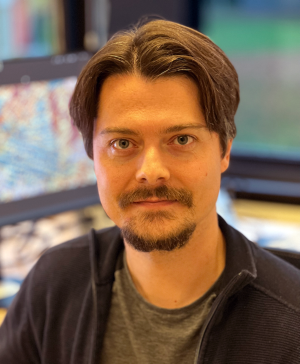
Dr.ir. Lars J. Bannenberg
Assistant Professor, Storage of Electrochemical Energy (SEE) group, Applied Sciences, Delft University of Technology
Title: X-ray and Neutron Diffraction and Reflectometry for (thin film) material characterization
The presentation is available here (Pdf file)
Abstract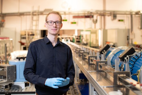 X-ray and neutron scattering techniques are invaluable probes to study the structure and composition of materials. Two of the most widely used techniques are diffraction and reflectometry. Whereas diffraction can be used to obtain information about the arrangement of atoms at the atomic scale, reflectometry can be used to obtain information on the composition, thickness and roughness of layered systems with a thickness in the ~1-300 nm range. Using (thin film) hydrogen sensing materials as an example, I will illustrate how neutron and X-ray diffraction and reflectometry provide complimentary information about the composition and structure of materials.
References
- Bannenberg, L., Schreuders, H., & Dam, B. (2021). Tantalum‐Palladium: Hysteresis‐Free Optical Hydrogen Sensor Over 7 Orders of Magnitude in Pressure with Sub‐Second Response. Advanced Functional Materials, 31(16), 2010483.
- Bannenberg, L. J., Schreuders, H., Kim, H., Sakaki, K., Hayashi, S., Ikeda, K., ... & Dam, B. (2021). Suppression of the Phase Coexistence of the fcc–fct Transition in Hafnium-Hydride Thin Films. The Journal of Physical Chemistry Letters, 12(45), 10969-10974.
- Morisset, A., Famprikis, T., Haug, F. J., Ingenito, A., Ballif, C., & Bannenberg, L. J. (2022). In Situ Reflectometry and Diffraction Investigation of the Multiscale Structure of p-Type Polysilicon Passivating Contacts for c-Si Solar Cells. ACS Applied Materials & Interfaces, 14(14), 16413-16423.
Dr. Antonija Grubišić-Čabo
Assistant Professor, Zernike Institute for Advanced Materials, Faculty of Science and Engineering, University of Groningen
Title: Angle-Resolved Photoemission Spectroscopy for crystalline (two-dimensional) material characterization
The presentation is available here (Pdf file, 86 MB)
 Abstract
Angle Resolved PhotoEmission Spectroscopy (ARPES) is a key technique for the investigation of the electronic structure of materials. The quality that separates ARPES from other surface science techniques is the direct visualisation of the electronic structure.
In this talk, I will introduce the technique and present data obtained on graphene, the quintessential two-dimensional material. This will include a discussion of the electronic structure characterization of graphene, band gap opening in graphene, as well as changes in the electronic structure of graphene due to physical structural modifications induced by intercalation.
I will also briefly showcase the possibilities of ARPES measurements performed on bulk materials.
References
- A. Grubišić-Čabo, J. C. Kotsakidis, Y. Yin, A. Tadich, M. Haldon, S. Solari, I. Di Bernardo, K. M. Daniels, J. Riley, E. Huwald, M. T. Edmonds, R. Myers-Ward, N. V. Medhekar, D. K. Gaskill, M. S. Fuhrer (2021). Magnesium-intercalated graphene on SiC: Highly n-doped air-stable bilayer graphene at extreme displacement fields, Applied Surface Science 541, 148612
- C. M. Polley, R. Buczko, A. Forsman, P. Dziawa, A. Szczerbakow, R. Rechciński, B. J. Kowalski, T. Story, M. Trzyna, M. Bianchi, A. Grubišić Čabo, P. Hofmann, O. Tjernberg, T. Balasubramanian (2018). Fragility of the Dirac cone splitting in topological crystalline insulator heterostructures, ACS Nano 12 (1), 617-626
- J. H. Jørgensen, A. Grubisic Cabo, R. Balog, L. Kyhl, M. N. Groves, A. M. Cassidy, A. Bruix, M. Bianchi, M. Dendzik, M. A. Arman, L. Lammich, J. I. Pascual, J. Knudsen, B. Hammer, P. Hofmann, L. Hornekaer (2016). Symmetry-driven band gap engineering in hydrogen functionalized graphene, ACS Nano 10 (12), 10798-10807
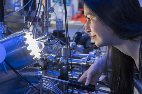
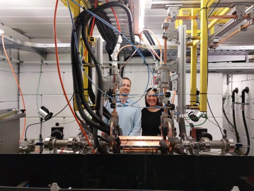
Dr. Gesa Welker (TU Delft) & Ir. Daniel Nijhof MSc (TU/e)
Postdoc in the Materials in Art and Archaeology group, Department of Materials Science and Engineering, Faculty 3mE, Delft University of Technology & PhD candidate in the Coherence and Quantum Technology group, Applied Physics, Eindhoven University of Technology
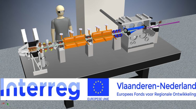
Topic: Smart*Light: A new type of X-ray source for materials characterization
The presentation is available here (8 MB)
 Abstract
X-rays are an invaluable tool for analyzing materials. Common X-ray sources in a laboratory environment are X-ray tubes, which are cost-efficient and compact, but produce incoherent X-rays with a broad bremsstrahlung continuum and characteristic lines at fixed energies with a low brilliance. Alternatively, synchrotron X-ray sources offer coherent, high brilliance light with a tunable energy, though only at large-scale research facilities. Such large facilities are very expensive in their operation, access for individual researchers is limited and the Netherlands have no stake in any of the international sources.
Smart*Light is a new type of X-ray source that combines the best of both worlds: It is a compact, coherent, high brilliance X-ray source with a tunable energy, fitting inside a normal laboratory. It is based on the principle of inverse Compton scattering, where photons from a laser collide with electrons, thereby shifting the energy of the photons into the X-ray regime.
Daniel Nijhof will present the current status of the Smart*Light setup located at Eindhoven University of Technology.
Gesa Welker will speak about the first experiments at Smart*Light, beam characterization and initial applications to the study of materials science samples, making use of X-ray fluorescence (XRF) and absorption imaging experiments.
Smart*Light
During the M2i Meeting Materials Conference, Smart*Light will also be present at the exhibition. Visit their booth to learn more about this new type of X-ray source for materials characterization.
M2i, the Materials innovation institute, is a partner in the Smart*Light program:
Transboundary research for highly innovative X-ray solutions
Chair of this session:

Header picture: Danqing Liu (TU/e) by Ernst de Groot (Communicating Surfaces)